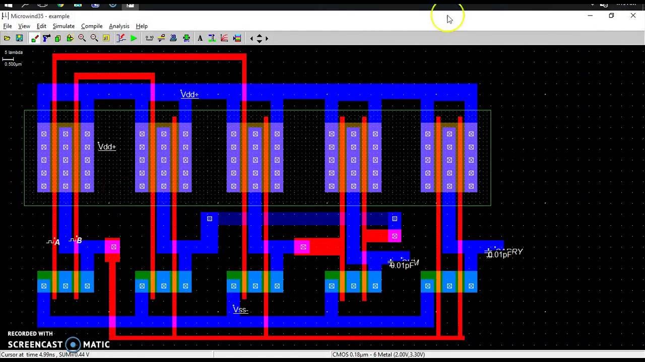
Design Full Adder Using Cmos
Cmos full adder design by 2x1 mux [11] Adder cmos 22nm Half adder using cmos
CMOS Full Adder Design [10] | Download Scientific Diagram
Low power-delay-product cmos full adder Cmos adder conventional Cmos adder
Cmos full adder design [10]
Tsmc 180 nm cmos full adder in lt spice measurement of delay and powerCommonly used bit full adder cells a conventional cmos full adder Full adder circuit – how it worksCmos half adder circuit diagram.
Electrical – cmos adder circuits – valuable tech notesDesign of cmos full adder || explore the way Tutorial on cmos vlsi design of a full adderAdder cmos existing.

Full adder
Snapshot of the cmos full adder designImplementation of low power 1-bit hybrid full adder using 22nm cmos Implemented half adder using cmos transmission gates [1].On the design of high-performance cmos 1-bit full adder circuits.
Layout of a 1 bit cmos full adder circuit download scCircuit diagram full adder using cmos High-gate-count full adder designs. (a) static cmos full adder8 bit adder subtractor circuit diagram.

Digital logic
Adder cmos 28tCmos half adder circuit diagram Conventional cmos full-adder, fa28tCmos fast-carry full adder.
Electrical – cmos adder circuits – valuable tech notesAdder cmos carry Schematic diagram of existing half adder using static cmos techniqueCircuit diagram full adder using cmos.

Circuit diagram half adder using cmos
Full adder using cmos logicCmos adder full vlsi Adder cmos mirror understand circuit stack works please help me logic pmos nmos network begingroupDesign full adder circuit using half adder.
Design of cmos half adder ||step by step process || explore the wayAdder sum simplified implementation logic combinational circuits Full adder cmos layoutConventional cmos full adder download high resolution.

3 bit full adder circuit diagram
.
.
![CMOS Full Adder Design By 2x1 Mux [11] | Download Scientific Diagram](https://i2.wp.com/www.researchgate.net/publication/260632302/figure/fig5/AS:342003033362440@1458551285582/CMOS-Full-Adder-Design-By-2x1-Mux-11.png)
![Implemented half adder using CMOS transmission gates [1]. | Download](https://i2.wp.com/www.researchgate.net/publication/354638199/figure/fig5/AS:11431281093206272@1667118330890/Half-Adder-Circuit-Diagram-Using-Conventional-Techniques-2_Q640.jpg)
Implemented half adder using CMOS transmission gates [1]. | Download
Circuit Diagram Full Adder Using Cmos

CMOS Fast-Carry Full Adder | Download Scientific Diagram

Electrical – CMOS Adder circuits – Valuable Tech Notes

On the Design of High-Performance CMOS 1-Bit Full Adder Circuits
![CMOS Full Adder Design [10] | Download Scientific Diagram](https://i2.wp.com/www.researchgate.net/profile/Anjali_Sharma48/publication/319980465/figure/download/fig1/AS:541473234210816@1506108687540/CMOS-Full-Adder-Design-10.png)
CMOS Full Adder Design [10] | Download Scientific Diagram

TSMC 180 nm CMOS Full Adder in LT Spice Measurement of Delay and Power